Connections & Ports
This page describes every external connector on the Lectron Jetson Autopilot baseboard, including its connector type, pin assignment, signal name and operating voltage.
The board is organized into two functional domains:
- Pixhawk FMU side — the flight-controller connectors that follow the Pixhawk Bus Standard (TELEMETRY, CAN, GPS, PWM, DEBUG, etc.).
- Jetson compute side — the Jetson module connectors (GPIO, SPI, UART, I2C, CSI CAMERA, CAN, Ethernet, USB, etc.).
Voltage Legend
Unless otherwise noted, all signal pins are +3.3V.
| Symbol | Meaning |
|---|---|
+5V |
High Power / Peripheral / System 5V rail |
+3.3V |
Logic-level signal (3.3V) |
+12/28V |
Main power input range |
0-16V |
Servo rail sense (depends on BEC) |
GND |
Ground |
--- |
Not connected / no defined level |
Warning
Most logic pins are 3.3V tolerant only. Do not apply 5V logic levels to signal pins, and never source servo/motor power from the peripheral 5V rail.
5V Power Output Limit
The board provides three independent 5V buses exposed at external connectors. Each bus is current-limited to 1.5 A. Do not exceed this limit across all peripherals connected to the same bus.
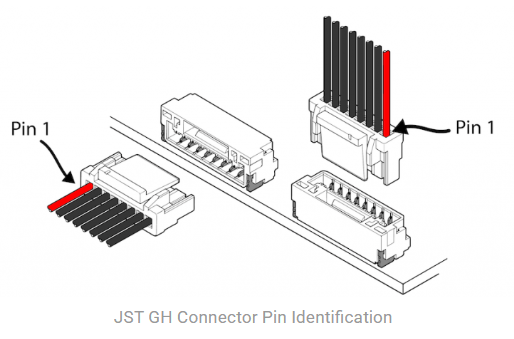
Pin 1 Identification
In every pinout table below, Pin 1 is the first row. Use the image below to locate Pin 1 on the physical JST GH connector before wiring.
FMU Connectors
Telemetry 1
Primary telemetry serial port with flow control (UART7) (BM06B-GHS).
| Pin | Signal | Voltage |
|---|---|---|
| 1 | HIGH POWER 5V | +5V |
| 2 | UART7 TX | +3.3V |
| 3 | UART7 RX | +3.3V |
| 4 | UART7 CTS | +3.3V |
| 5 | UART7 RTS | +3.3V |
| 6 | GROUND | GND |
Telemetry 2
Secondary telemetry serial port with flow control (UART5) (BM06B-GHS).
| Pin | Signal | Voltage |
|---|---|---|
| 1 | PERIPHERAL 5V | +5V |
| 2 | UART5 TX | +3.3V |
| 3 | UART5 RX | +3.3V |
| 4 | UART5 CTS | +3.3V |
| 5 | UART5 RTS | +3.3V |
| 6 | GROUND | GND |
Telemetry 3
Tertiary telemetry serial port with flow control (USART2) (BM06B-GHS).
| Pin | Signal | Voltage |
|---|---|---|
| 1 | PERIPHERAL 5V | +5V |
| 2 | USART2 TX | +3.3V |
| 3 | USART2 RX | +3.3V |
| 4 | USART2 CTS | +3.3V |
| 5 | USART2 RTS | +3.3V |
| 6 | GROUND | GND |
CAN
Primary CAN bus for the flight controller (BM04B-GHS).
| Pin | Signal | Voltage |
|---|---|---|
| 1 | PERIPHERAL 5V | +5V |
| 2 | CAN HIGH | +3.3V |
| 3 | CAN LOW | +3.3V |
| 4 | GROUND | GND |
FMU Debug
SWD + serial debug for the FMU processor (SM10B-SRSS).
| Pin | Signal | Voltage |
|---|---|---|
| 1 | FMU VDD 3.3V | +3.3V |
| 2 | USART3_TX_DEBUG | +3.3V |
| 3 | USART3_RX_DEBUG | +3.3V |
| 4 | FMU_SWDIO | +3.3V |
| 5 | FMU_SWCLK | +3.3V |
| 6 | NC | |
| 7 | NFC_GPIO | +3.3V |
| 8 | PH11 | +3.3V |
| 9 | FMU_NRST | +3.3V |
| 10 | GROUND | GND |
IO Debug
SWD + serial debug for the IO co-processor (SM10B-SRSS).
| Pin | Signal | Voltage |
|---|---|---|
| 1 | IO VDD 3.3V | +3.3V |
| 2 | IO_USART1_TX_DEBUG | +3.3V |
| 3 | NC | --- |
| 4 | IO_SWDIO | +3.3V |
| 5 | IO_SWCLK | +3.3V |
| 6 | IO_SWO | +3.3V |
| 7 | NC | |
| 8 | NC | |
| 9 | IO_NRST | +3.3V |
| 10 | GROUND | GND |
GPS-1 (FULL)
Full GPS port with safety switch, LED and buzzer outputs (BM10B-GHS).
| Pin | Signal | Voltage |
|---|---|---|
| 1 | PERIPHERAL 5V | +5V |
| 2 | USART1 TX | +3.3V |
| 3 | USART1 RX | +3.3V |
| 4 | I2C1 SCL | +3.3V |
| 5 | I2C1 SDA | +3.3V |
| 6 | SAFETY SWITCH IN | +3.3V |
| 7 | SAFETY LED OUT | +3.3V |
| 8 | FMU 3.3V | +3.3V |
| 9 | BUZZER(-) | +3.3V |
| 10 | GROUND | GND |
GPS-2 (BASIC)
Secondary GPS port (serial + I2C only) (BM06B-GHS).
| Pin | Signal | Voltage |
|---|---|---|
| 1 | HIGH POWER 5V | +5V |
| 2 | UART8 TX | +3.3V |
| 3 | UART8 RX | +3.3V |
| 4 | I2C2 SCL | +3.3V |
| 5 | I2C2 SDA | +3.3V |
| 6 | GROUND | GND |
SBUS
RC receiver input (PPM/SBUS) with RSSI feedback (BM05B-GHS).
| Pin | Signal | Voltage |
|---|---|---|
| 1 | PERIPHERAL 5V | +5V |
| 2 | PPM INPUT / SBUS INPUT | +3.3V |
| 3 | NC | --- |
| 4 | RSSI IN / SBUS OUTPUT | +3.3V |
| 5 | GROUND | GND |
DSM Support
The Lectron Jetson Autopilot product doesn't support DSM.
FMU USB
USB 2.0 Type-C for firmware flashing and MAVLink over USB (USB 2.0 Type-C).
| Pin | Signal | Voltage |
|---|---|---|
| - | - | 5V |
IO PWM (MAIN)
Main PWM outputs driven by the IO co-processor (BM10B-GHS).
| Pin | Signal | Voltage |
|---|---|---|
| 1 | VDD SERVO SENS | 0-16V |
| 2 | IO PWM CH1 | +3.3V |
| 3 | IO PWM CH2 | +3.3V |
| 4 | IO PWM CH3 | +3.3V |
| 5 | IO PWM CH4 | +3.3V |
| 6 | IO PWM CH5 | +3.3V |
| 7 | IO PWM CH6 | +3.3V |
| 8 | IO PWM CH7 | +3.3V |
| 9 | IO PWM CH8 | +3.3V |
| 10 | GROUND | GND |
FMU PWM (AUX)
Auxiliary PWM outputs driven directly by the FMU (BM10B-GHS).
| Pin | Signal | Voltage |
|---|---|---|
| 1 | VDD SERVO SENS | 0-16V |
| 2 | FMU PWM CH1 | +3.3V |
| 3 | FMU PWM CH2 | +3.3V |
| 4 | FMU PWM CH3 | +3.3V |
| 5 | FMU PWM CH4 | +3.3V |
| 6 | FMU PWM CH5 | +3.3V |
| 7 | FMU PWM CH6 | +3.3V |
| 8 | FMU PWM CH7 | +3.3V |
| 9 | FMU PWM CH8 | +3.3V |
| 10 | GROUND | GND |
Warning
Do not apply servo sense voltage above 16V.
I2C3
I2C3 peripheral bus (BM04B-GHS).
| Pin | Signal | Voltage |
|---|---|---|
| 1 | PERIPHERAL 5V | +5V |
| 2 | I2C3 SCL | +3.3V |
| 3 | I2C3 SDA | +3.3V |
| 4 | GROUND | GND |
UART4
UART4 peripheral port (BM04B-GHS).
| Pin | Signal | Voltage |
|---|---|---|
| 1 | PERIPHERAL 5V | +5V |
| 2 | UART4 TX | +3.3V |
| 3 | UART4 RX | +3.3V |
| 4 | GROUND | GND |
External Power Sensor Input
External power module / battery monitoring (I2C1) (SM04B-GHS).
| Pin | Signal | Voltage |
|---|---|---|
| 1 | SYSTEM 5V 1 | +5V |
| 2 | I2C1 SCL | +3.3V |
| 3 | I2C1 SDA | +3.3V |
| 4 | GROUND | GND |
Jetson Connectors
Jetson GPIO
General-purpose I/O header (SM10B-GHS).
| Pin | Signal | Voltage |
|---|---|---|
| 1 | SYSTEM 5V | +5V |
| 2 | JETSON GPIO00 | +3.3V |
| 3 | JETSON GPIO01 | +3.3V |
| 4 | JETSON GPIO02 | +3.3V |
| 5 | JETSON GPIO03 | +3.3V |
| 6 | JETSON GPIO05 | +3.3V |
| 7 | JETSON GPIO07 | +3.3V |
| 8 | JETSON GPIO10 | +3.3V |
| 9 | JETSON GPIO11 | +3.3V |
| 10 | GROUND | GND |
Jetson SPI
SPI0 bus with single chip-select (SM06B-GHS).
| Pin | Signal | Voltage |
|---|---|---|
| 1 | SYSTEM 5V | +5V |
| 2 | JETSON SPI0 SCK | +3.3V |
| 3 | JETSON SPI0 MISO | +3.3V |
| 4 | JETSON SPI0 MOSI | +3.3V |
| 5 | JETSON SPI0 CS0 | +3.3V |
| 6 | GROUND | GND |
Jetson UART0
General-purpose serial port (SM04B-GHS).
| Pin | Signal | Voltage |
|---|---|---|
| 1 | SYSTEM 5V | +5V |
| 2 | JETSON UART0 TX | +3.3V |
| 3 | JETSON UART0 RX | +3.3V |
| 4 | GROUND | GND |
Jetson UART1
General-purpose serial port (SM04B-GHS).
| Pin | Signal | Voltage |
|---|---|---|
| 1 | SYSTEM 5V | +5V |
| 2 | JETSON UART1 TX | +3.3V |
| 3 | JETSON UART1 RX | +3.3V |
| 4 | GROUND | GND |
Jetson UART2 (Debug)
Serial debug console (SM03B-GHS).
| Pin | Signal | Voltage |
|---|---|---|
| 1 | JETSON UART2 TX | +3.3V |
| 2 | JETSON UART2 RX | +3.3V |
| 3 | GROUND | GND |
Jetson I2C0
I2C0 peripheral bus (SM04B-GHS).
| Pin | Signal | Voltage |
|---|---|---|
| 1 | SYSTEM 5V | +5V |
| 2 | JETSON I2C0 SCL | +3.3V |
| 3 | JETSON I2C0 SDA | +3.3V |
| 4 | GROUND | GND |
Jetson I2C1
I2C1 peripheral bus (SM04B-GHS).
| Pin | Signal | Voltage |
|---|---|---|
| 1 | SYSTEM 5V | +5V |
| 2 | JETSON I2C1 SCL | +3.3V |
| 3 | JETSON I2C1 SDA | +3.3V |
| 4 | GROUND | GND |
System Ethernet 1
Differential Ethernet pairs (SM04B-GHS).
| Pin | Signal | Voltage |
|---|---|---|
| 1 | ETH1 TXP | --- |
| 2 | ETH1 TXN | --- |
| 3 | ETH1 RXP | --- |
| 4 | ETH1 RXN | --- |
System Ethernet 2
Differential Ethernet pairs (SM04B-GHS).
| Pin | Signal | Voltage |
|---|---|---|
| 1 | ETH2 TXP | --- |
| 2 | ETH2 TXN | --- |
| 3 | ETH2 RXP | --- |
| 4 | ETH2 RXN | --- |
Jetson CSI-1 — Camera
15-pin 1mm-pitch FPC carrying CSI port 3 plus camera control (15-pin FPC (1mm)).
| Pin | Signal | Voltage |
|---|---|---|
| 1 | GROUND | GND |
| 2 | CSI3_D0_N | +3.3V |
| 3 | CSI3_D0_P | +3.3V |
| 4 | GROUND | GND |
| 5 | CSI3_D1_N | +3.3V |
| 6 | CSI3_D1_P | +3.3V |
| 7 | GROUND | GND |
| 8 | CSI3_CLK_N | +3.3V |
| 9 | CSI3_CLK_P | +3.3V |
| 10 | GROUND | GND |
| 11 | CAM1_PWDN | +3.3V |
| 12 | CAM1_MCLK | +3.3V |
| 13 | JN_CAM_I2C_SCL 2 | +3.3V |
| 14 | JN_CAM_I2C_SDA 2 | +3.3V |
| 15 | SYSTEM 3.3V | +3.3V |
Jetson CSI-2 — Camera
15-pin 1mm-pitch FPC carrying CSI port 0 plus camera control (15-pin FPC (1mm)).
| Pin | Signal | Voltage |
|---|---|---|
| 1 | GROUND | GND |
| 2 | CSI0_D0_N | +3.3V |
| 3 | CSI0_D0_P | +3.3V |
| 4 | GROUND | GND |
| 5 | CSI0_D1_N | +3.3V |
| 6 | CSI0_D1_P | +3.3V |
| 7 | GROUND | GND |
| 8 | CSI0_CLK_N | +3.3V |
| 9 | CSI0_CLK_P | +3.3V |
| 10 | GROUND | GND |
| 11 | CAM0_PWDN | +3.3V |
| 12 | CAM0_MCLK | +3.3V |
| 13 | JN_CAM_I2C_SCL 2 | +3.3V |
| 14 | JN_CAM_I2C_SDA 2 | +3.3V |
| 15 | SYSTEM 3.3V | +3.3V |
Jetson CAN (SPI Interfaced)
CAN bus via an MCP2515 controller on SPI0-CS1 (SM04B-GHS).
| Pin | Signal | Voltage |
|---|---|---|
| 1 | SYSTEM 5V | +5V |
| 2 | CAN HIGH | +3.3V |
| 3 | CAN LOW | +3.3V |
| 4 | GROUND | GND |
Jetson Fan 1
PWM-controlled cooling fan with tachometer feedback (SM04B-SRSS).
| Pin | Signal | Voltage |
|---|---|---|
| 1 | SYSTEM 5V | +5V |
| 2 | JETSON PWM (INVERTED) | +3.3V |
| 3 | GROUND | GND |
| 4 | JETSON TACHO 3 | +3.3V |
Jetson Fan 2
PWM-controlled cooling fan (no tacho) (SM04B-SRSS).
| Pin | Signal | Voltage |
|---|---|---|
| 1 | SYSTEM 5V | +5V |
| 2 | JETSON PWM (INVERTED) | +3.3V |
| 3 | GROUND | GND |
| 4 | NC 4 | --- |
Shared PWM Signal
Both fans are driven by the same PWM source. They cannot be controlled independently.
Jetson USB 3.0
USB 3.0 Type-C host port (USB Type-C).
| Pin | Signal | Voltage |
|---|---|---|
| - | - | +5V |
Jetson USB 2.0 (Debug)
USB 2.0 Mini debug port (USB Mini).
| Pin | Signal | Voltage |
|---|---|---|
| - | - | +5V |
Jetson SD Card
MicroSD slot (TF SD Card).
| Pin | Signal | Voltage |
|---|---|---|
| - | - | +3.3V |
System Power
General 12V Out
Regulated 12V output stepped down from the main power input, current-limited to 2A — designator U1 (SM04B-GHS).
| Pin | Signal | Voltage |
|---|---|---|
| 1 | SYSTEM 12V | +12V |
| 2 | SYSTEM 12V | +12V |
| 3 | GROUND | GND |
| 4 | GROUND | GND |
Power Input (XT30)
Main board power input (XT30).
| Pin | Signal | Voltage |
|---|---|---|
| 1 | 12-28V INPUT | +12/28V |
| 2 | GROUND | GND |
Power Input
Observe correct polarity on the XT30 input. Input voltage must stay within +12V to +28V; reverse polarity or over-voltage may permanently damage the board.
Use the Supplied XT30 Cable Only
Power the board exclusively through the XT30 cable supplied by Lectron. Using a third-party or incorrectly wired cable may damage the onboard regulator stage. This cable compansate voltage ripples that are caused by motors.
Reference
Connector layout follows the Pixhawk Bus Standard on the FMU side.